Numerically Controlled Oscillator
To generate a waveform, the VCO is substituted by a Numerically Controlled Oscillator (NCO) [1]. Its design consists of two parts:
- A phase accumulator (PA), which is basically a counter incremented by a reference clock
- A phase-to-amplitude converter, which uses the PA output as an index to a Look-Up Table (LUT)
Let’s imagine now that the vector skips a few (fixed) points for each jump, the revolution is completed in a much shorter time: the frequency of the output waveform has increased!
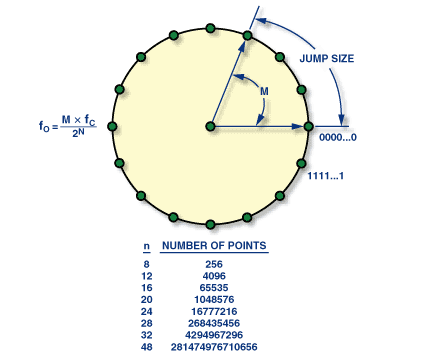
Fig. 2 The phase wheel
The correlation between the jump size, the reference clock and the output waveform frequency is
\(f_{OUT} = \frac{M \times f_C}{2^n}\)
where:
- \(M\) is the jump size
- \(f_{OUT}\) is the NCO output waveform frequency
- \(f_C\) in the reference clock frequency
- \(n\) is the length of the phase accumulator, in bits
To retrieve a digital clock signal, the LUT is actually very simple: we just associate to half of the circle the digital value 0, and to the other half the digital value 1.
The design presents two main limitations:
- The first is the maximum frequency limit, which is given by Nyquist, and corresponds to half of the reference clock
- The second is the phase resolution. Since the output signal is digital, the time domain is discrete, and it corresponds to the reference clock period. This implies that the positive (and negative) fraction of the output clock signal can only be a multiple of this time domain resolution, making the output frequency only on average determined by the jump size of the accumulator.
While the first limitation is known and impossible to overcome, the second is design based, and must be resolved in order to be able to use this clock for CDR operations.
Phase resolution increase
The NCO output clock will still present differences between the average frequency value and the istantaneous frequency value (the time domain is still descrete, we just reduced its period), but this can be filtered out feeding the signal to an FPGA’s MMCM/PLL, in jitter filter mode.
| [1] | https://www.analog.com/en/analog-dialogue/articles/all-about-direct-digital-synthesis.html |