Top level
file: top_cdr_fpga.vhd
The file top_cdr_fpga.vhd is the top level file for the CDR project.
For an easier code comprehension it is recommended to have the CDR documentation and code on the side.
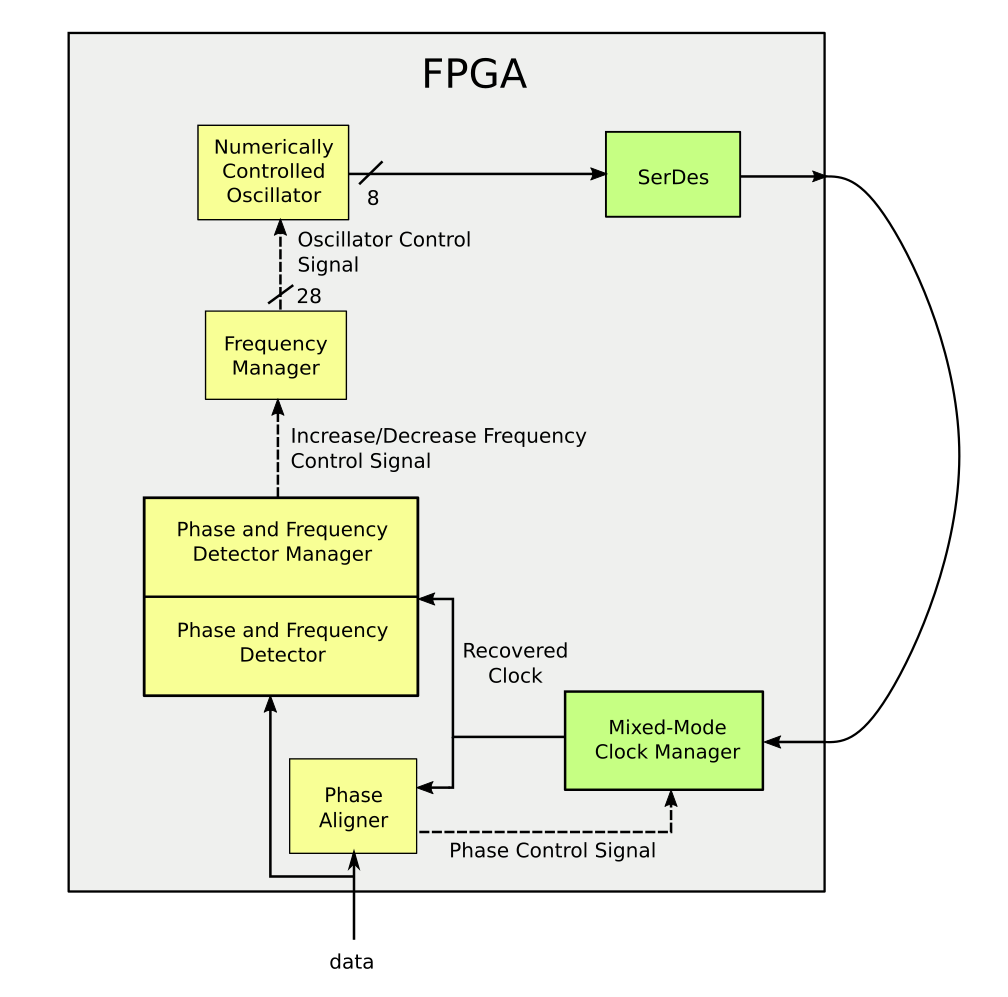
Fig. 5 Block level for the CDR proposed project
The generic and ports used by the CDR design are:
- g_gen_vio: boolean, when “true” the Xilinx VIO is generated, whose ports are used to make the NCO generate a fixed clock frequency (M_i) and to enable the phase and frequency detector (vio_DMTD_en)
- g_check_jc_clock: boolean, when “true” the recovered clock is forwarded out to the differential pin cdrclk_jc_p/n_o
- g_check_pd: boolean, when “true” some internal signals are forwarded out from the FPGA in order to be checked (with an oscilloscope for istance). Used for debug purposes.
- g_number_of_bits: positive, this defines the number of bits used by the NCO’s phase wheel. The number of bits determine the NCO’s output frequency resolution
- g_multiplication_factor: positive number which is needed to have an output frequency higher than the maximum obtainable frequency of the single phase wheel (due to Nyquist law). The user only need to make sure that \(g\_freq\_out / 2^{g\_multiplication\_factor - 1} < g\_freq\_in / 2\)
- g_freq_in: real, system clock frequency (i.e., the frequency of the clock that enters the i_phase_wheel_counter_1 instance), in MHz
- g_freq_out: real, NCO nominal output frequency (i.e., the data rate), in MHz
- g_out_phase: recovered cloc - data phase relationship
- sysclk_p/n_i: clock from the board crystal
- data_to_rec_i: data from which the clock is recovered
- cdrclk_p/n_o: NCO’s generated clock which has gone through the OSERDESE2 tile and need an external loopback
- cdrclk_p/n_i: clock is going back in from the loopback
- cdrclk_jc_p/n_o: if enabled, this differential pins shows the recovered clock
- ledx_o: several LED showing whether the MMCM are locked, if data is entering the FPGA and if the NCO’s clock is actually present
- shifting_o, shifting_en_o: debug ports
On the report, a block diagram of the CDR design is reported. The corresponding istances in the top level code are:
- Numerically Controlled Oscillator <=> i_phase_wheel_counter_1
- Frequency Manager <=> i_frequency_manager_1
- SerDes <=> i_oserdese_manager_1
- Mixed-Mode Clock Manager <=> i_jitter_cleaner_1, i_i_q_cloc_gen_1
- Phase and Frequency Detector <=> i_pfd_1
- Phase and Frequency Detector Manager <=> i_pfd_manager_1, i_lock_manager_1
- Phase Aligner <=> i_phase_detector_unit_1
Some of these istances will have its code explained here.
Other notable istances are: i_slow_pulse_counter which is used to show a defined LED pulse based on data rate, PRBS_ANY_1 which is a PRBS checker, i_prbs_counter_1 which is a counter of PRBS errors.