Introduction
The Clock and Data Recovery job is a relatively simple one: retrieve a clock with the frequency needed to sample each bit of the incoming data stream.
Its design, unfortunately, is not so trivial.
Usually a CDR architecture is similar to the Phase Locked Loop (PLL) model (Fig. 1), where the phase of a reference signal is compared to the phase of an adjustable feedback signal, generally provided by a Voltage Controlled Oscillator (VCO). The output of the Phase Detector (PD) is filtered and used to pilot the VCO frequency. When the phase comparison is in steady state, e.g. the phase and frequency of the reference signal is equal to the phase and frequency of the feeedback signal, we say that the PLL is locked.
In the case of a CDR, the steady state is reached when the VCO clock frequency match the reference signal’s data rate.
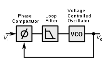
Fig. 1 Basic design of a PLL.
Essentially, breaking down the design, for a fully functional CDR, a controlled oscillator and a PD are needed.
This paper has the intent to show a possible implementation of a CDR. .. adopting the FPGA technology, in particular the target is a Xilinx Kintex 7 (XC7K325T–2FFG900C), which presents a good balance between performances and cost. In particular the target is a Xilinx Kintex 7 (XC7K325T-2FFG900C). The design is intended to work with a range of data rates that allows the use of the high range (HR) general purpose I/O pin of the FPGA over the dedicated tranceivers, resulting in a reduced power consumption and a more straightforward design.